
Personal profile
暂未填写

发布时间:2025-05-09
文章标题:Nanoscale Horizons: Optoelectronic synapses realized on large-scale continuous Te doped MoSe2
内容: https://doi.org/10.1039/D5NH00062A Synaptic devices with integrated sensing–computing–storage functions are emerging as promising technological solutions to break the memory wall in the von Neuman architecture computing system. 2D semiconductors are ideal candidate materials for artificial synapses due to their superior electronic and optoelectronic properties. In this work, we report robust optoelectronic synapses realized on wafer-scale continuous MoSe2 with Te-doping-induced tunable memory functions. A unique defect engineering strategy of substitutional doping of Te has been adopted to induce Se vacancies in chemical vapour deposition grown MoSe2 films. These vacancies introduce defect states as deep trap levels in the band gap, enabling efficient charge trapping and significantly prolonging the decaying time. The presence of Te doping and Se vacancies was confirmed by PL, Raman, and XPS characterization. Ultra-high vacuum stencil lithography technique has been adopted for the fabrication of arrayed optoelectronic devices that exhibit prominent excitatory postsynaptic currents with the paired-pulse facilitation up to 197% under ultraviolet illumination. Therefore, essential synaptic behaviors like the spike-number-, spike-rate-, and spike-intensity-dependent plasticity have been demonstrated, along with the in-sensor computation application of hardware image sharpening capability. This work offers a new method of vacancy engineering in large-scale 2D semiconductors for future application in integrated neuromorphic devices. 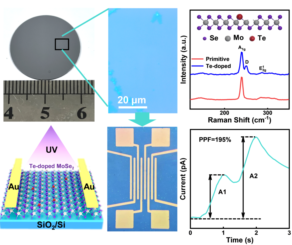
版权所有:西安交通大学 陕ICP备05001571号