Personal profile
暂未填写

发布时间:2025-02-26
文章标题:ACS ami: Surface Argon Plasma Treatment Enabled Broadband Optoelectronic Synapses
内容: ACS Appl. Mater. Interfaces 2025 doi:10.1021/acsami.4c22477 Creating and tuning charge trapping states by introducing atomic-scale defects are crucial for the optoelectronic synapses that parallelize sensing, processing, and memorizing of optical signals in a single device, which is essential for bioinspired neuromorphic computing. Herein, a mild Ar-plasmatreatment approach to enable synaptic behavior in 2D semiconductor devices has been proposed and demonstrated in large-scale epitaxial GaSe GaN heterostructures. The GaSe films were epitaxially grown on a GaN substrate by physical vapor deposition in an ultrahigh vacuum environment, while the devices were fabricated in situ using a shadow mask-assisted electrode deposition technique. A tailored mild Ar-plasma treatment on the GaSe films has been employed to create atomic-scale defects, which provide charge trapping states in the band gap without making morphological damage, as confirmed by the Raman spectra, scanning electron microscopy, and photoluminescence characterizations. Optoelectronic transport measurement under pulsed illumination of varying wavelengths reveals broadband photoresponse and significantly prolonged response time (×103) that give rise to the superior performance of the synaptic devices. This has been proven by the simulation of classic synaptic behaviors of adaptive pain perception and associative learning. Our work provides an efficient approach to facilitate optoelectronic synaptic behaviors in 2D semiconductor devices. This work was mainly carried out by Yunan Lin, who is currently a Master student.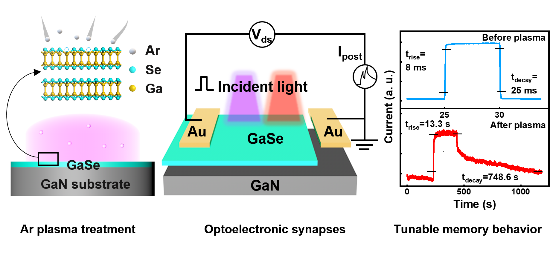
版权所有:西安交通大学 陕ICP备05001571号